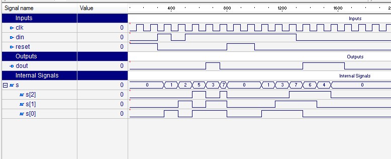
8 Bit Serial To Parallel Converter Verilog Code
In general a shift register is characterized by the following control and data. Synchronous/asynchronous parallel load; clock enable; serial or parallel output. 8-bit Shift-Left Register with Positive-Edge Clock, Serial In, and Serial Out. Following is the Verilog code for an 8-bit shift-left register with a negative-edge clock,. Oct 17, 2010 - Popular Posts. 8-bit Shift-Left/Shift-Right Register with Positive-Edge Clock, Serial In, and Parallel Out---->VHDL & Verilog. IO Pins Description.
Hello I am trying to implement a parallel in serial out shift register based on the data sheet for the 74LV165A 8 bit parallel in serial out shift register the spec sheet may be found at If I make my test bench begin by shifting in serially, then try to latch data on the parallel input the data does not appear. If I begin the test bench in with parallel latch enabled then the data appears on the Q and will clock through once shifting is enabled. My goal is to shift several sets of data through this register however currently this behavior is preventing this. Any help would be very very appreciated, event if its just a hint:) Currently I am monitoring the set and reset information and the Q lines.
Parallel-in/ serial-out shift registers do everything that the previous serial-in/ serial-out shift registers do plus input data to all stages simultaneously. The parallel-in/ serial-out shift register stores data, shifts it on a clock by clock basis, and delays it by the number of stages times the clock period. In addition, parallel-in/ serial-out really means that we can load data in parallel into all stages before any shifting ever begins. This is a way to convert data from a parallel format to a serial format.
By parallel format we mean that the data bits are present simultaneously on individual wires, one for each data bit as shown below. By serial format we mean that the data bits are presented sequentially in time on a single wire or circuit as in the case of the “data out” on the block diagram below. Below we take a close look at the internal details of a 3-stage parallel-in/ serial-out shift register. A stage consists of a type for storage, and an AND-OR selector to determine whether data will load in parallel, or shift stored data to the right. In general, these elements will be replicated for the number of stages required.
How to download ps2 pfs explorer files to my device? Click download file button or Copy ps2 pfs explorer URL which shown in textarea when you clicked file title, and paste it into your browsers address bar. If file is multipart don't forget to check all parts before downloading! Put a browser windows-explorer-like styled for The two sides (PC files to PS2 PFS system); Set Drag and Drop to work properly. Set and make multiple files work properly (1 drag to various files at the same time) Manage PFS HDD Partitions (A function like WinHip`s formating HDD, and Explore ALL partitions like in the listing function of PFSShell). Software ps2 pfs explorer.
We show three stages due to space limitations. Four, eight or sixteen bits is normal for real parts. Above we show the parallel load path when SHIFT/LD’ is logic low.
The upper NAND gates serving D A D B D C are enabled, passing data to the D inputs of type D Flip-Flops Q A Q B D C respectively. At the next positive going clock edge, the data will be clocked from D to Q of the three FFs. Three bits of data will load into Q A Q B D C at the same time. The type of parallel load just described, where the data loads on a clock pulse is known as synchronous load because the loading of data is synchronized to the clock.
This needs to be differentiated from asynchronous load where loading is controlled by the preset and clear pins of the Flip-Flops which does not require the clock. Only one of these load methods is used within an individual device, the synchronous load being more common in newer devices. The shift path is shown above when SHIFT/LD’ is logic high. The lower of the pairs feeding the are enabled giving us a shift register connection of SI to D A, Q A to D B, Q B to D C, Q C to SO. Clock pulses will cause data to be right shifted out to SO on successive pulses.
The waveforms below show both parallel loading of three bits of data and serial shifting of this data. Parallel data at D A D B D C is converted to serial data at SO. What we previously described with words for parallel loading and shifting is now set down as waveforms above.
As an example we present 101 to the parallel inputs D AA D BB D CC. Next, the SHIFT/LD’ goes low enabling loading of data as opposed to shifting of data. It needs to be low a short time before and after the clock pulse due to setup and hold requirements.  It is considerably wider than it has to be. Though, with synchronous logic it is convenient to make it wide. We could have made the active low SHIFT/LD’ almost two clocks wide, low almost a clock before t 1 and back high just before t 3. The important factor is that it needs to be low around clock time t 1 to enable parallel loading of the data by the clock.